- 您现在的位置:买卖IC网 > Sheet目录340 > MAX15025EATB+T (Maxim Integrated)IC GATE DRVR 2CH 16NS 10TDFN-EP
�� �
�
�MAX15024/MAX15025�
�Single/Dual,� 16ns,� High� Sink/Source�
�Current� Gate� Drivers�
�Power� Dissipation�
�Power� dissipation� of� the� MAX15024/MAX15025� con-�
�sists� of� three� components:� the� quiescent� current,�
�capacitive� charge� and� discharge� of� internal� nodes,� and�
�the� output� current� (either� capacitive� or� resistive� load).�
�The� sum� of� these� components� must� be� kept� below� the�
�maximum� power-dissipation� limit.� The� quiescent� cur-�
�rent� is� 700μA� typ.� The� current� required� to� charge� and�
�discharge� the� internal� nodes� is� frequency� dependent�
�(see� the� Typical� Operating� Characteristics� ).� The�
�MAX15024/MAX15025� power� dissipation� when� driving�
�a� ground-referenced� resistive� load� is:�
�P� =� D� x� R� ON(MAX)� x� I� LOAD2�
�where� D� is� the� fraction� of� the� period� the� MAX15024/�
�MAX15025s’� output� pulls� high,� R� ON(MAX)� is� the� maxi-�
�mum� on-resistance� of� the� device� with� the� output� high�
�(p-channel),� and� I� LOAD� is� the� output� load� current� of� the�
�MAX15024/MAX15025.� For� capacitive� loads,� the� power�
�dissipation� for� each� driver� is:�
�P� =� C� LOAD� x� V� DRV2� x� FREQ�
�where� C� LOAD� is� the� capacitive� load,� V� DRV� is� the� driver�
�supply� voltage,� and� FREQ� is� the� switching� frequency.�
�Layout� Information�
�The� MAX15024/MAX15025� MOSFET� drivers� source� and�
�sink� large� currents� to� create� very� fast� rise� and� fall� edges�
�at� the� gate� of� the� switching� MOSFET.� The� high� di/dt� can�
�cause� unacceptable� ringing� if� the� trace� lengths� and�
�impedances� are� not� well� controlled.� The� following�
�printed-circuit� board� (PCB)� layout� guidelines� are� recom-�
�mended� when� designing� with� the� MAX15024/MAX15025:�
�?� Place� one� or� more� 1μF� decoupling� ceramic� capaci-�
�tor(s)� from� V� DRV� to� PGND� as� close� to� the� device� as�
�possible.� At� least� one� storage� capacitor� of� 10μF� (min)�
�should� be� located� on� the� PCB� with� a� low� resistance�
�path� to� the� V� CC� pin� of� the� MAX15024/MAX15025.�
�?� There� are� two� AC� current� loops� formed� between� the�
�device� and� the� gate� of� the� MOSFET� being� driven.�
�The� MOSFET� looks� like� a� large� capacitance� from�
�gate� to� source� when� the� gate� is� being� pulled� low.�
�The� active� current� loop� is� from� MOSFET� gate� to�
�OUT_� of� the� MAX15024/MAX15025� to� PGND� of� the�
�MAX15024/MAX15025,� and� to� the� source� of� the�
�MOSFET.� When� the� gate� of� the� MOSFET� is� being�
�pulled� high,� the� active� current� loop� is� from� the� V� DD�
�terminal� of� the� V� DRV� terminal� of� decoupling� capaci-�
�tor,� to� the� V� DRV� of� the� MAX15024/MAX15025,� to� the�
�OUT_� of� the� MAX15024/MAX15025,� to� the� MOSFET�
�gate,� to� the� MOSFET� source,� and� to� the� negative� ter-�
�minal� of� the� decoupling� capacitor.� Both� charging�
�current� loop� and� discharging� current� loop� are� impor-�
�tant.� It� is� important� to� minimize� the� physical� distance�
�and� the� impedance� in� these� AC� current� paths.�
�?� Keep� the� device� as� close� as� possible� to� the� MOSFET.�
�?� In� the� multilayer� PCB,� the� inner� layers� should� consist�
�of� a� GND� plane� containing� the� discharging� and�
�charging� current� loops.�
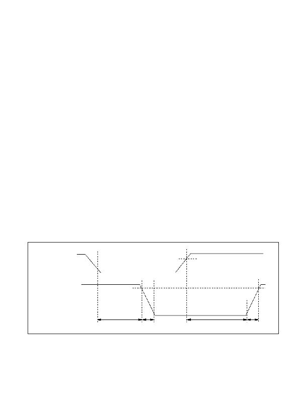
�IN+�
�V� IH�
�V� IL�
�P_OUT� AND�
�N_OUT� CONNECTED�
�TOGETHER�
�OR� OUT1/OUT2�
�90%�
�10%�
�t� D-OFF�
�t� F�
�t� D-ON�
�t� R�
�Figure� 1.� Timing� Diagram�
�Maxim� Integrated�
�11�
�发布紧急采购,3分钟左右您将得到回复。
相关PDF资料
MAX15053EVKIT+
BOARD EVAL FOR MAX15053
MAX15054AUT+T
IC MOSFET DVR HIGH SIDE SOT-23-6
MAX15070BEUT+T
IC MOSFET DRIVER HNM LL SOT23-6
MAX15103EVKIT#
EVAL KIT MAX15103
MAX1554ETA+T
IC LED DVR WHITE BCKLGT 8TDFN
MAX1570ETE+
IC LED DRVR WHITE BCKLGT 16-TQFN
MAX1573ETE+
IC LED DRVR WHITE BCKLGT 16-TQFN
MAX1574ETB+T
IC LED DRVR WHITE BCKLGT 10TDFN
相关代理商/技术参数
MAX15025FATB+T
功能描述:功率驱动器IC Dual Low Side RoHS:否 制造商:Micrel 产品:MOSFET Gate Drivers 类型:Low Cost High or Low Side MOSFET Driver 上升时间: 下降时间: 电源电压-最大:30 V 电源电压-最小:2.75 V 电源电流: 最大功率耗散: 最大工作温度:+ 85 C 安装风格:SMD/SMT 封装 / 箱体:SOIC-8 封装:Tube
MAX15025GATB+T
功能描述:功率驱动器IC Dual Low Side RoHS:否 制造商:Micrel 产品:MOSFET Gate Drivers 类型:Low Cost High or Low Side MOSFET Driver 上升时间: 下降时间: 电源电压-最大:30 V 电源电压-最小:2.75 V 电源电流: 最大功率耗散: 最大工作温度:+ 85 C 安装风格:SMD/SMT 封装 / 箱体:SOIC-8 封装:Tube
MAX15025HATB+T
功能描述:功率驱动器IC Dual Low Side RoHS:否 制造商:Micrel 产品:MOSFET Gate Drivers 类型:Low Cost High or Low Side MOSFET Driver 上升时间: 下降时间: 电源电压-最大:30 V 电源电压-最小:2.75 V 电源电流: 最大功率耗散: 最大工作温度:+ 85 C 安装风格:SMD/SMT 封装 / 箱体:SOIC-8 封装:Tube
MAX15026AEUD+
制造商:Maxim Integrated Products 功能描述:SINGLE/DUAL, 16NS, HIGH SINK/SOURCE CURRENT GATE DRIVERS - Rail/Tube
MAX15026BATD+
制造商:Maxim Integrated Products 功能描述:- Rail/Tube
MAX15026BATD+T
功能描述:DC/DC 开关控制器 4.5-28V Synchronous Buck Controller RoHS:否 制造商:Texas Instruments 输入电压:6 V to 100 V 开关频率: 输出电压:1.215 V to 80 V 输出电流:3.5 A 输出端数量:1 最大工作温度:+ 125 C 安装风格: 封装 / 箱体:CPAK
MAX15026BETD/V+
制造商:Maxim Integrated Products 功能描述:LOW-COST, SMALL, 4.5V TO 28V WIDE OPERATING RANGE, DC-DC SYN - Rail/Tube
MAX15026BETD/V+T
制造商:Maxim Integrated Products 功能描述:LOW-COST, SMALL, 4.5V TO 28V WIDE OPERATING RANGE, DC-DC SYN - Tape and Reel